







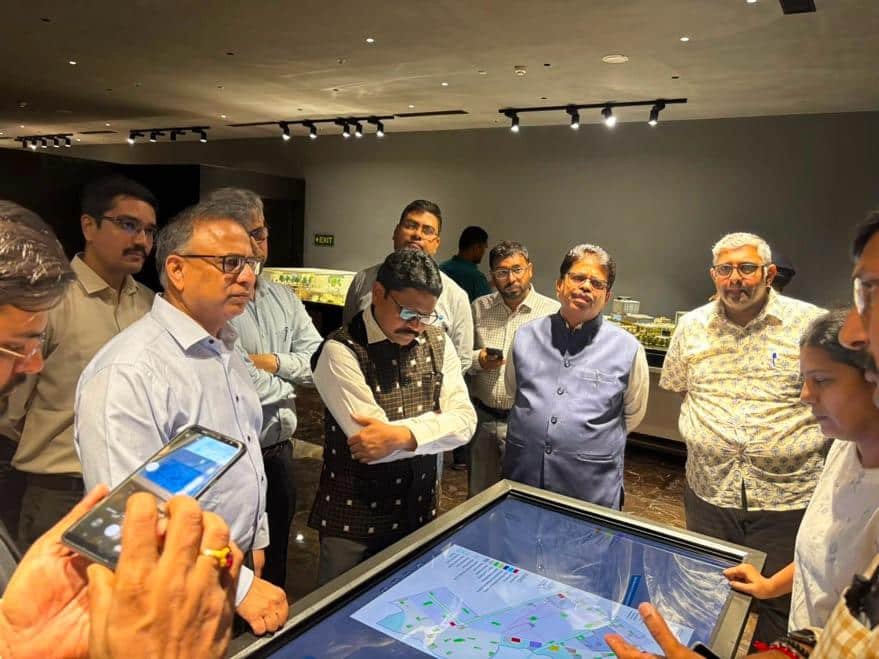
In a strategic move to establish Odisha as a significant player in India’s semiconductor and technology sector, Electronics and IT Minister Dr. Mukesh Mahaling has recently concluded a crucial visit to Gujarat’s Dholera Special Investment Region and the semiconductor fabrication facility of Tata Electronics.
During his visit, the minister examined Dholera’s integrated industrial framework and its model for urban development, focusing particularly on the activation area. The impressive scale of the modern township design, along with its plug-and-play infrastructure and future-ready utilities, provided valuable insights that Odisha could implement in its forthcoming industrial corridors.
Additionally, Dr. Mahaling toured the Tata Electronics semiconductor fabrication plant, gaining direct knowledge about the intricate requirements involved in chip manufacturing. After the visit, he emphasized a vital point: “Establishing a fab is merely the first step. Developing a complete semiconductor ecosystem requires a strong vendor network, high-quality infrastructure, skilled workforce, and a conducive policy environment. This visit has equipped us with essential insights that will directly inform Odisha’s semiconductor strategy.”
The minister asserted that with the visionary leadership of Prime Minister Narendra Modi and the dedicated guidance of Chief Minister Mohan Charan Majhi, Odisha is poised to become the country’s next significant semiconductor and technology hub by effectively blending modern infrastructure, cutting-edge technology, and a dynamic industrial ecosystem.
Among the senior officials who accompanied the minister were Additional Chief Secretary (Electronics & IT) Vishal Kumar Dev, OPTCL Chairman Bhaskar Jyoti Sharma, OCAC CEO Dr. Pradeep Kumar Rout, Joint Secretary Kaustuv Pani, and other departmental representatives.
This visit signifies Odisha’s commitment to evolving beyond traditional industries, actively positioning itself as a key contributor to India’s semiconductor initiative.