


Bookings for Odisha’s 3D semiconductor chip plant are already in place even before construction begins, signaling strong early demand in a tough sector. Even before the first structure has come up, demand is already locked in. That’s what makes Odisha’s new semiconductor project stand out; not just another foundation stone ceremony, but a plant whose future output has effectively been spoken for. And that, more than the speeches, is what’s getting attention.
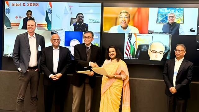
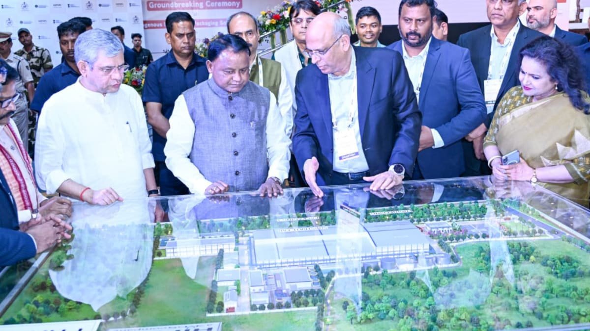
On Sunday, Chief Minister Mohan Charan Majhi and Union IT Minister Ashwini Vaishnaw laid the foundation for US-based 3D Glass Solutions Inc’s advanced chip packaging unit in Bhubaneswar’s Info Valley. The pitch is ambitious: bring some of the most advanced packaging technology into India, and in the process, move the country a step higher in the global chip value chain.
But here’s the unusual bit. According to officials, bookings for the plant’s production have already been made ahead of construction. In a sector where projects often struggle to secure demand early on, that flips the usual script.
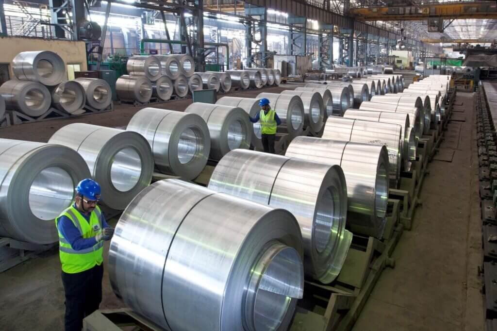
The facility itself isn’t a traditional semiconductor fab. It focuses on advanced packaging — specifically 3D glass substrate technology — which is increasingly critical for high-performance chips used in artificial intelligence, defence systems, and high-speed computing.
Most chip manufacturing still relies on silicon substrates. This plant will use glass instead, allowing for more efficient layering and integration of components — the kind of architecture newer AI workloads demand. It’s also the first time this technology is being deployed at scale in India.
Planned capacity gives a sense of the scale: roughly 70,000 glass panels, 50 million assembled units, and over 13,000 3D heterogeneous integration modules annually. The investment is pegged at around Rs 2,000 crore, with commercial production expected to begin by 2028.
For Odisha, the shift is as significant as the technology itself. The state has traditionally leaned on minerals and metals. This project, along with another approved semiconductor unit, signals a push into electronics and high-end manufacturing. The government is framing it as the beginning of a broader transition — from a resource-based economy to one tied to advanced tech.
There’s also the jobs angle. Officials estimate over 2,000 direct employment opportunities once the plant is operational, with a wider ecosystem likely to follow.
Still, timelines in semiconductor projects are long, and India has seen big-ticket announcements before that didn’t quite materialise as planned. This one, though, comes with a few differences: confirmed demand, backing from global investors linked to companies like Intel and Lockheed Martin, and a clear focus on next-generation packaging rather than conventional assembly.
Zoom out, and the context becomes clearer. India has approved 10 semiconductor-related projects with investments crossing Rs 1.6 lakh crore. The larger goal is to reduce dependence on imports and build a domestic ecosystem — not just in fabrication, but across the value chain.
Packaging, often overlooked, is a crucial piece of that puzzle. It’s where chips are assembled, optimised, and prepared for real-world use. And increasingly, it’s where innovation is happening. That’s why this Odisha plant matters beyond state lines. It’s not just about adding capacity. It’s about where that capacity sits in the global hierarchy — and whether India can move from being a consumer of chips to playing a more meaningful role in how they’re built. For now, the strongest signal isn’t the technology or the investment number. It’s the fact that buyers are already in line.